Design and Growth of Quantum Materials
|
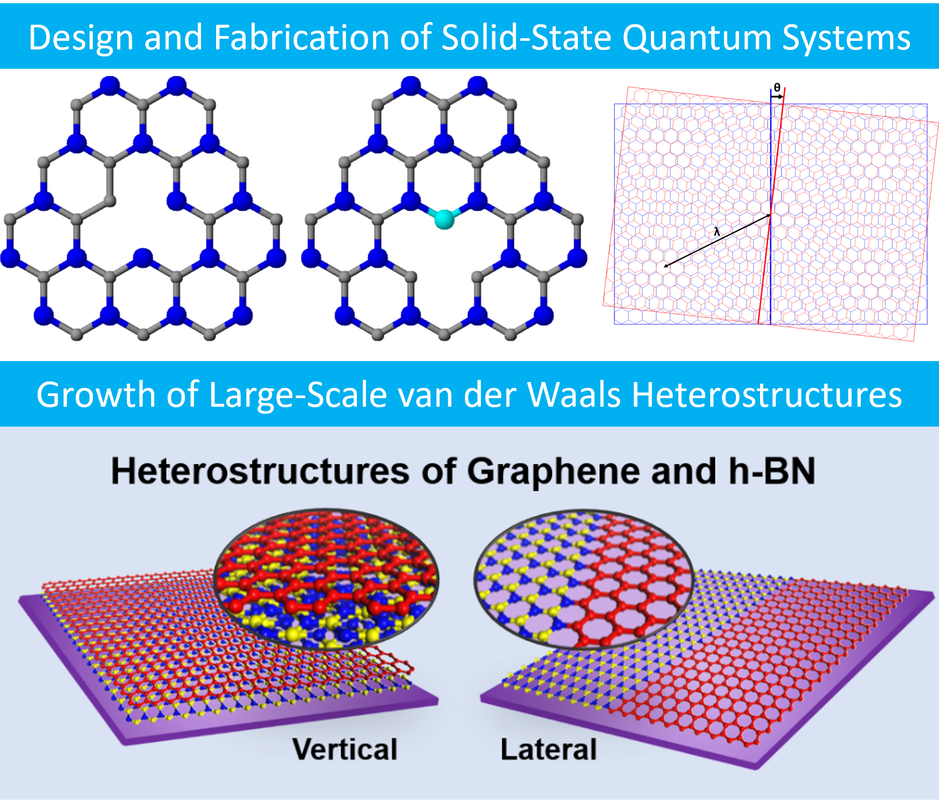
Creating solid-state quantum light sources hosted on the surface of the material in contrast to the defect-based sources buried within the bulk of the material is promising for quantum sensing and quantum networking. In this regard, atom-thin 2D quantum materials are truly surfaces and they have unique chemical structures, robust mechanical flexibility, and novel electronic and optical properties. Behura Research Group is creating solid-state quantum optical sources in 2D and moiré materials. We also realize that these materials are prepared through either exfoliation from bulk crystals or synthesized on catalytic metal surfaces. Both approaches impose severe processing constraints hindering the integration of quantum light sources into photonic circuitry. The Behura Group is developing new atomic-scale synthesis chemistries to directly nucleate wide bandgap 2D materials and moiré superlattices.
|
Optoelectronic Characterization
|
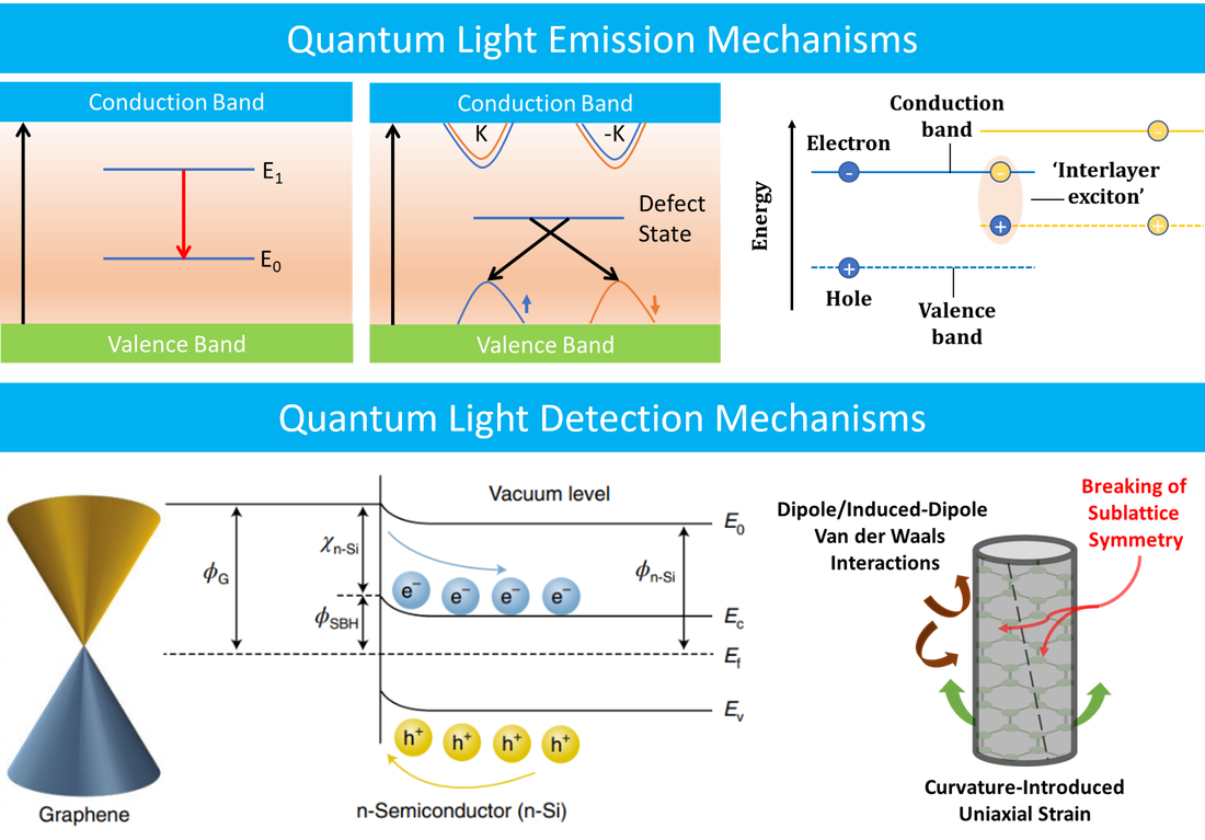
Designer materials provide on-demand quantum states due to strongly correlated quantum interactions. Probing these quantum states is critical for the development of quantum technologies. The Behura Research Group is developing a complete optoelectronic characterization toolbox including cryo-magnetic Raman, Photoluminescence (PL), Photon Emission Correlation Spectroscopy, Photocurrent Imaging, and Time Correlated Photon Counting. These characterization tools will be employed to study the quantum emission phenomena of non-classical light in solid-state materials. The group is also developing light-sensitive, mixed-dimensional 'surface junction - only one-atom below the front surface' as quantum light detector.
|
Quantum Control Science and Engineering
|
The accelerated development of quantum information science is becoming relevant for room temperature operation of quantum technologies such as quantum computing and quantum sensing. The spin-optical properties of two-dimensional (2D) quantum emitters enable single photons as quantum bits (qubits). In this regard, a single boron vacancy defect of hexagonal boron nitride (h-BN) such as point defect can be made into a room temperature qubit since the large bandgap of h-BN (6 eV) can shield a computational subspace from environmental noise. To design high quality photonic qubits, dynamical simulation that incorporates noise and radiative-like decay is needed to optimize quantum control schemes for h-BN. We develop a model of the spin active defect Hamiltonian from material properties including key coupling tensors such as zero field splitting, Zeeman effect, and hyperfine splitting.
|